JHS Overdrive Clone Build
On Friday 2nd October 2020 JHS launched their brand new 3 Series Pedal line. On the 7th October Josh, and the team, did a live stream for Sweetwater where they demoed these. During that stream Josh showed the schematics for all 7 of these new pedals and said the following:
Here's the schematic to this pedal. You can screenshot it, make it your self. We do not care.
So screen shot it I did, and so began my journey cloning a brand new pedal.
Schematic
The first job was to copy the schematic out from an iPad screen shot into something I can use. I used KiCad for this project as it’s open source (so free), reasonably well documented and fairly easy to use. This is the same software I used for my Katana 50 controller build.
This wasn’t too hard to do, the screen shot was pretty clear and so it was just a case of copying what I saw. A quick trip into Photoshop and some un-sharp mask helped reading a capacitor value and cropped off the black borders.
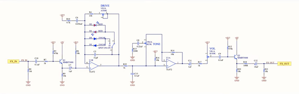
The diagram Josh showed didn’t have any power section however. As such I designed my own based on some previous experience and a Brian Wampler book I have which suggested 2 power filter caps, I was only going to add the single 47uF. The design also called for 4.5V in some places. I did this with a simple potential divider circuit. I wasn’t sure on what values to use for this but some quick research seemed to show that 10K was fine so I went with that. A Klon uses 27K, so I think I am probably in the right ball park here.
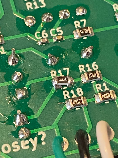
There is an error in this schematic, R17 should be 100R not 100K See the Update section below.
PCB Design
Ominous warning: this isn’t all true by the end of our journey.
This bit is a lot harder. For this build I decided to try use some surface mount parts for the first time and get these assembled at the manufacturer. What was to be SMD and what I would add later was decided on a part by part basis.
Almost all caps are to be soldered on as I chose to get name brand (Wima poly and Panasonic electrolytic) parts from RS Components, 2 caps are SMD mainly as I was finding them hard to source. C5/C6 are “extended” parts which means a £3 charge each to load less common parts them the machine. This sounds expensive but a Mica 51pF for C6 is £1.42 each and I’d need to order 50. Or pay the £3 and they cost £0.0092 each after that.
Resistors are all SMD to save space and build time. I wouldn’t expect them to affect the sound adversely as they are commonly used in modern production pedals, including those made by JHS. The hardest part was figuring out what wattage to go for. Handily JHS quote a 12mA draw on the pedal giving 0.108W @ 9V. So a 1/8W should be fine as no single resistor has a full draw through it but leaves some headroom incase I am wrong.
All the diodes are SMD, mainly for size reasons but it also saves some build time and are a little cheaper that way.
The 2 transistors are SMD, as thats what an MMBT5088 is.
Finally I went for named Alpha 9mm pots and an RS pro switch to avoid nasty stuff from eBay and also mean I should be able to depend on them in future if I like them.
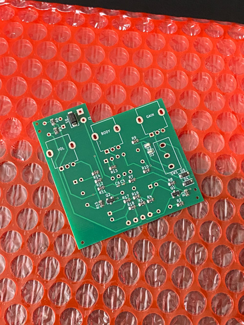
With all my parts chosen the I was able to select the correct footprints for them in Kicad. The software just dumps them into a mess on a new pcb, it’s completely unusable like this. My wife spent at least 30 minuted just dragging stuff apart so it was a bit more clear what we had to work with.
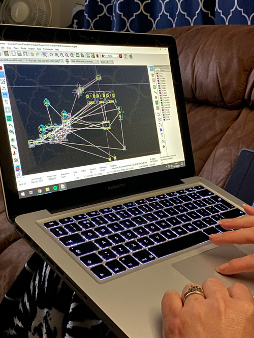
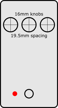
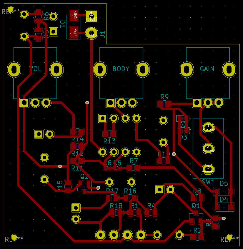
First job was to position the pots and switches as these are pretty limited to where they can go. I used an old 1590B knock off I had to get some measurements and drew it up in Inkscape with the 3 knobs and the switch. It was quite obvious the knobs would need to be no bigger than about 18mm or they just wouldn’t fit or be usable. After a bit of tweaking I was happy a 19.5mm spacing for the pots and positioned them on the PCB.
To add the switch I needed to first create a footprint for it. Whilst RS provide one it’s not compatible with KiCad, so I used the data sheet and created my own. This isn’t too hard and is quite quick to do. With this done I just dropped it in centred on the gain pot and as close as seemed sensible for a nice look. I also positioned the input, output and power connections for the switch at the bottom to match the daughter board I had previously bought from fuzz dog.
The actual layout was just a case of putting things where they might make sense, then trying to wire stuff up. If it didn’t work I’d clear all the wires move some bits and try again. As things began to firm up I would lock them in place1 which stops you moving them by accident, and also means you they aren’t cleared by default when you delete all. Slowly but surely you end up with most things connected and after a final push with some vias I was able to connect everything.
I am pretty sure that if the fine people at JHS saw my routing they would be horrified. I found the SMD parts made things harder as all the SMD parts need to be on the same face (a limit from the manufacturer). As there are no through holes I couldn’t just run lines one which ever side made more sense, but I got there in the end with some vias.
I did try keep to some general rules I am aware of, don’t run stuff parallel if possible, the 9V and 4v5 lines do for a while but I think this will be okay, make wires cross at 90° and generally try not to shove too much into a small area. I also added a large ground plane to the bottom side which I hope will help with noise reduction.
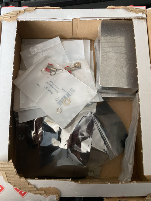
PCB Manufacture
I went with JLCPCB again to get the PCBs, but have added a few options. I am going for lead free boards and also removing their order tracking number. Sadly as I am going for SMD assembly I can only select a green board, not black like I wanted.
Getting the boards made is just a case of following their guides on the web site. They have guides specifically for KiKad for both the boards and assembly stages.
There are a few extra steps needed for assembly that I didn’t need for just ordering blank boards. First you need to export a BOM, a positions file, and also you need to add some small holes2 to the board for location during assembly. This is all documented in the help and is quite easy to do, if a little time consuming.
Manufacturing was a fair bit slower than my previous order. I clearly hit a busy patch.
A Problem
Before I get into the “how it was made” and “does it work” bit a brief note that shows I don’t really know what I am doing and you shouldn’t really be listening to me. I was reading a pedal breakdown, and noticed a 47uF capacitor from the 4.5V to ground in the power supply. I don’t have one. I checked a few pedals: Boss DS-1, Ibanez Tubscreamer, Klon Centaur. All of them have this 47uF cap in the 4.5V supply.
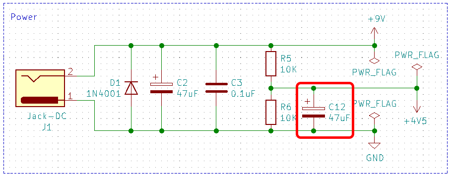
Apparently this is a decoupling capacitor which is there to deal with voltage spikes or dropouts and also reduces the impedance (which is sort of like resistance but for AC and I am struggling to understand). Clearly this is something that I should have added as it’s a common feature, but alas, the boards were made before I noticed, but before they arrived. Looking at the boards I am able to add in a capacitor from pin 1 of the volume pot to the closest ground pin. Obviously this isn’t ideal but it’s also something I’ve seen in real products where something was missed out in early revisions.
Assembly
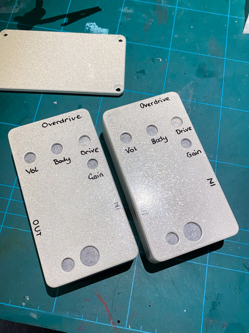
First job is drilling out the enclosure. Masking tape is applied to protect it and then careful measurements are needed to get everything in the right spot. Easier said than done, and things are a bit tight. I did some tests on an old scrap enclosure to help check things and then made a few minor adjustments for the ones I will be using. I wasn’t sure on what jack I would be using due to space so this scrap test was useful in trying to get things to fit. I also drill all the holes around 1mm over size, especially the pots and switch. This gives a small amount of wiggle room if you’re not spot on when drilling by hand.
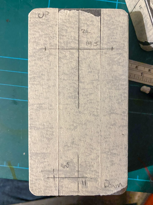
With everything marked out I carefully centre punch each hole. First is a 2mm drill, then a 4mm drill. Finally a step drill is used to get each hole to final size. These range from 7-12mm. The enclosures are painted and labeled before final assembly. I also cleaned the paint from one of the screw holes on the base plate with a drill bit, this will help ensure a solid electrical join between the cases for shielding. I probably didn’t need to as I masked off the joining faces but some paint did get in under it.
I normally use 60/40 leaded solder as I find it easier to solder with. For this project I am using lead free, I have some from previous projects, one is a standard type the other has some silver in it. The goal being these are ROHS compliant, not that I need to worry about this as a hobbyist. I went with some by Rapid Electronics, with my iron set to 350ºC this worked better than any other lead free I’ve used and was actually similar to the leaded solder I have.
First I soldered the daughter boards to the foot switches and tested them with a multi meter for continuity. Essentially check the jack in goes to jack out, then click the switch and jack in should go to circuit in and circuit out to jack out.
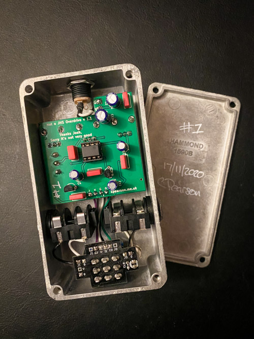
The I added all the film capacitors first, followed by the electrolytics taking care of the polarity. As I need to add on the missing coupling capacitor later I left the ground leg on C2 to help attach it later. After the capacitors were on I added the socket for the op-amp. As the legs are very short this is a bit fiddly but bending each corner holds it well enough to solder without too much movement.
The switch came next. The legs on this are not going to bend to help hold it while soldering. By luck the holes I designed were snug enough to hold it if I set the board vertical in the holder to do the first pin, before turning it over to finish the rest.
Last up, the pots. The side support pins were problematic and didn’t fit through the holes. A minor nudge with some pliers was needed to bring them in a little before they would fit. On one I slightly over adjusted the legs. On this one I applied solder to one support, then whilst holding the iron in place pushed the pot into place before removing the iron while still holding it. This held the pot nicely allowing me to solder it in with out it moving.
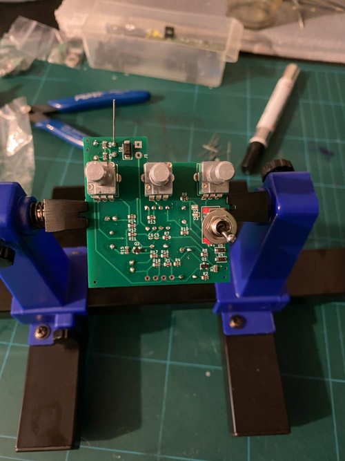
The missing cap was added by adding it between the C2 47uF filter cap ground leg and pin 1 on the volume pot. The legs were covered in insulation stripped from some hookup wire. Very fiddly but did the job.
For the second board, rinse and repeat.
A bigger problem, much bigger.
Boards complete I added the switch assembly, temporarily added the power jack and plugged in before casing up. Clean tone, so the switch is fine, awesome. Click Nothing. Click Click Still nothing, uh oh.
Out came the multi meter, power was getting where it needed and at the right voltages. Maybe I have the OpAmp in backwards, flip, nope still nothing. Dead op amp? pulled it out, left it on the socket, grabbed a new one, went to move the old one thats HOT3. So that one’s definitely dead, but the new one also does nothing. Eventually looking at the board I notice that the 9V pin for the MMBT5088s seems oddly placed. I load up the data sheet and sure enough it’s because it’s wrong. I had 9V going straight into the base, and the other two were wrong as well, every single pin was in the wrong pad.
Being SMD parts, thats it we’re done. No fancy solder work will save the day here as the pads are just too small.
How did this happen? Generic footprints. The part uses a SOT-23 package, and I assumed that pin 1 on an SOT-23 would always be the same. Not so, when compared to the schematic what pins 1-3 meant for my chosen part didn’t tie up to the generic SOT-23 footprint.
This shows the default vs a version edited so that they matched the layout of the selected part.
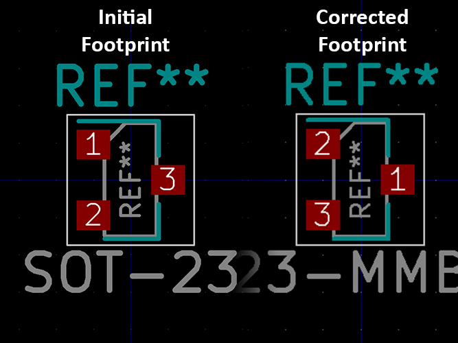
With the boards updated with the correct footprint, and triple checked against the datasheet I went order some new PCBs.
Only there was a problem. The MMBT5088s are no longer available from JLCPB. Whilst I could carry on and buy some cheaply enough there was no way I was hand soldering SMD parts, my soldering is no where near good enough. Fortunately the datasheet gave the through hole part number, 2N5088, and my favorite part vendor stocks them. So another foot print swap, some minor layout changes and triple check later I was back to waiting for PCBs to be made.
Did it work?
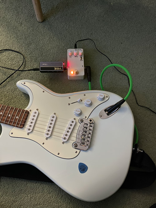
With the new boards in hand I built up one, lesson learnt this time. Before boxing up I clipped a 9V battery on to the power terminals and tentatively plugged in my Vox AmPlug 2 Clean and grabbed my daughters Epiphone Les Paul SL as it was to hand. It worked!
That was enough initial testing so I boxed up the board, and found I’d cut the wires to the foot switch too short. Measure once, cut twice 📏✂️✂️. This was a pain as I’d already had to remove the link wires from this switch once from the first build, and didn’t fancy doing it again because os a silly mistake. With that fixed I went and plugged in my S-500. And it sounded great, but was rather quiet.
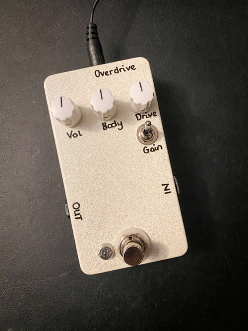
The volume really wants to be turned up pretty much full to even get unity. The gain control works well bringing in more or less grit as you play with it. I’ve not spent a huge amount of time with it but it’s certainly a promising sounding pedal. There’s plenty of range in the gain, and the switch does add 2 different flavours.
So what went wrong with the volume? I am not sure4. My gut wants to say it’s an issue with the 4.5V supply, but it give 4.8V when plugged into a wall adapter, half the 9.3V that gives out. Maybe that’s the issue and it’s causing some bias issues, but the components there are as per the JHS schematic so their pedal would surely have the same issue (which would have ben mentioned in reviews, and wasn’t).
There is also a chance the swap from MMBT5088 to 2N5088 may have needed a changes to the R4 & R16 resistors and are actually not acting as unity buffers? Ultimately I am now far outside of my comfort zone.
I feel at this point the project is done. Whilst not perfect I have learnt a lot and do have a usable pedal, despite the flaws.
I still have the 2nd enclosure, so maybe I’ll return to it the project one day and try and bread board the pedal and see if I can figure out what I did wrong.
Lessons learnt
During this project I’ve learnt a few things and there are a number of things I would do differently.
Firstly, and sort of a big one: check your pin layouts when using a generic footprint for a part. This ended up loosing me 5 PCBs and SMD parts, and 2 more boards worth of board mounted parts including the switches and pots which ended up being quite an expensive loss.
Another big one is I didn’t research my power section enough. Reading through some pedal breakdowns after I ordered the PCBs I quickly noticed the issue and so I should have looked at some other pedals for examples rather than using the basic one in the Wampler book. This would have saved some stress but ultimately was fixed in the 1.1 boards so I “got away with it”.
I didn’t think enough about the specs of the components I chose. The electrolytic caps are all over spec’d for voltage significantly. One is rated for 250V when 25V would have been enough. Again this was resolved in the 1.1 board where smaller electrolytic caps were used.
The toggle switch also falls into this area, I opted for a micro toggle switch. I later discovered sub-micro switches which would have been a smaller footprint and often have stubby toggles which would have been a better fit for this use case. Though these often don’t use a securing nut which I am using to hide my sins from the drilling. I didn’t update this for 1.1 as I had bought enough for the 2nd version and didn’t want to buy more.
I also didn’t take enough care about leaving space for the footswitch and the jacks. Whilst I was careful about space for the power jack I just didn’t apply the same care for the rest. This lead to issues getting my primary choices into the enclosure. In future I would spend the time to make out the whole inside of the enclosure when designing the PCB, perhaps going as far as to design my own daughter board and PCB mounting both the foot switch and jacks more like a production pedal.
Grounding, I also didn’t think about how to ground the enclosure at all. If I had stuck with the REAN NYS229 jacks I was originally going to use this would have been done via the jacks. However I ended up swapping to Neutrik NMJ4HC-S which are isolated jacks. This means I had to fine an alternative way to do this. I ended up adding a wire from a spare Ground hole and wrapped it under the bottom nut on the foot switch. Not ideal but it grounds the enclosure, and so should be helping to reduce noise. Definitely something to pay more attention to in future builds.
Not so much a lesson but an observation. Drilling the enclosures is tricky by hand, no matter how much care you take they end up a little bit off. Ideally I’d like a drill press to help keep the bit straight to the enclosure which should help keep them where I want them.
Worth it?
Well, actual cash money? 1 pedal is quite a lot cheaper if you get it right the first time. But I screwed up and lost 2 full pedals worth of components and 5 boards all went in the bin, something like £30 went into a black bag. Had I got it right, then building one would be cheaper than buying one but I didn’t. So it would have been cheaper to just buy the stupid pedal, and it would have worked better.

Parts for 1 pedal are around £39, but that’s just the parts used. You have to order PCBs in units of 5, I ordered extras of most/all parts so I could make mistakes, which I did so they were used up and can’t be saved for future projects. I could have saved a few £ here and there by just making the one for a start, or using cheaper caps etc. Ultimately the raw costs for a low volume run (of 2) add up fast and saving 6p on a capacitor or 20p on a jack socket isn’t going to change that. You really need to be making enough to hit some price breaks which will bring costs down per unit.
What’s not factored in here is my time. I spent between 3 and 4 hours copying the schematic and the checking it. I don’t know how long I spent on the PCB layout but it was 2-3 evenings. I am also not counting the time spent looking at data sheets or looking up help docs on what I needed to get the boards fabbed or all kinds of time I spent on this.
Also not included is equipment. I have a soldering iron, PCB holders, drill, drill bits, measuring equipment etc. If you don’t you’re going to need to buy them, I got some extra equipment to make this build easier. And that adds up quite quickly I can assure you.
In all this was a lot of work to do.
That said this was never about saving money on a pedal. This was about learning more about electronics, and building pedals. I don’t overly like fuzz or vero board which are the usual starting points. These cheaply made China made PCBs have made this a much more interesting way for a single builder to get started and learn in something that is closer to what the pro’s are doing. Yes it’s a bit slow, but if you just want PCBs you can have them in your hands in in a few days if you pay for good shipping.
This is where it gets awkward. I don’t know how much of the $/£99 JHS get but they £0.00 on these. That’s no contribution to wages, equipment, facilities, R&D, Josh’s pedal collection. Nothing. Whilst I can’t see me making a pair of these causing them to go out of business if everyone did, they would and we’d all be poorer for it.
Normally for my projects I throw them up on github or something so others can use them. I am not doing that with this. I would feel like I am making it too easy for you. If you want to make a “cheap” Overdrive, the above tells you how I did it. Now you go do it. If you don’t want to work for it then please buy one from Andertons | Sweetwater | Amazon. The first two aren’t affiliate links, that Amazon one is.
JHS did the actual work on these, so please pay them for it.
Thanks Josh for the schematic and the permission to build one. This was a fun project and a welcome distraction from this year.
Update!
Updated 18/08/2021
Recently I was browsing Pedal PCB looking for a schematic to clarify against another project and saw they now did a clone of this very pedal. Given the issues I had I grabbed the schematic and compared it to mine to try and see where I went wrong.
The power supply was similar to my v1.1 version, slightly different values for the splitter and the 4.5v decoupling cap. What was very different was what I have as R17 and is R18 on the original schematic JHS posted.
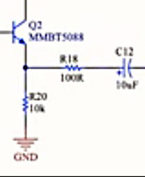
In my schematic R17 is a 100k resistor, they have a 100R or 100 ohm. So my value is 1000x bigger than it should be in the output path! No wonder it was so quiet.
This was fixable, though it did mean learning to solder SMD parts. So after a lot of time on Youtube and a few days for the SMD resistors to arrive I was ready to fix it.
Removing the old part is simple. Take a hot soldering iron and hold it at one end for a while, then push. The heat will have heated the whole resistor so the solder at both ends melts and makes it easy to remove. Next I cleaned up with a little flux and some solder wick to get rid of the old solder and leave a nice flat surface to work on.
Soldering on the new 0805 resister is less easy and took some practice. Fortunately I still had some of the old v1.0 boards which I could use to get the hang of things.
The rough plan is apply a small blob of solder to one side, then push the resistor into this and reflow the solder with your iron. With any luck this sucks the part into place. Then you finish off by soldering the 2nd side. It’s not easy and my result wasn’t perfect but it worked.
With the part replace the pedal finally behaved as you would expect! The volume has a nice usable range and no longer needs to be maxed to be useful. The two clipping modes have very different characters, I found I preferred the LED mode with the gain at around 1 o’clock and then the volume lowered to around 9 o’clock to keep it at around unity.
Whilst the pedal works now it was all still a bit of an anti-climax. The pedal is nice but the process to get to the end has been “less than ideal”.
-
Select the item them press L. You can multi-select items with shift which makes locking in traces and blocks of components easier. ↩
-
I must have got this wrong as JLCPCB added more pre-manufacture. For V1.1 I just left them off and let JLC add them. ↩
-
Pro tip: when removing an IC from a socket, REMOVE IT. Don’t leave it sat on the socket so who knows what pins connect to who knows what on the socket. This can make them hot. Also, throw that hot IC in the bin, not randomly on the bench. So when you then go to clean up you don’t end up with 2 identical chips, one is probably dead, and no way to tell them apart. ↩
-
Maybe it’s actually fine and my Amplug is not liking it. I’ve not had time to setup my Boss Katana 50 yet as I only really get my lunch breaks to work on this at the moment. ↩